Frequently Asked Questions
InterFET’s main focus is JFET based products! We are committed to delivering JFET solutions when others are discontinuing their products. InterFET Corporation has gained the reputation of providing the best JFETs for many specialty applications requiring very low noise performance. This is supported by recommendations from scientists at Lawrence Berkeley National Laboratory, Brookhaven National Laboratory, and various universities working with low-noise electronics. InterFET is mentioned by name in the literature for many experiments conducted at CERN, Fermi Labs, and the former Superconducting Super-Collider project. Most of these applications gain enhanced noise performance by operation at cooled temperatures, which often reveals the purity of the materials and processes used in the construction of the JFET. This is very important to noise performance, a key attribute of junction FETs.
InterFET FAQs
- Founded in 1982 as a spinoff from Texas Instruments Silicon Small Signal Group
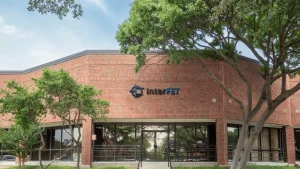
- Located in Richardson Texas
- Focuses on JFET based products
- World’s Largest Standard JFET line available
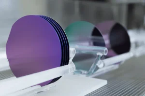
- Multiple outsourced Wafer Fab locations
- Both in-house and outsourced assembly and testing
- Worldwide rep structure to support our customers wherever they are located
- Majority of InterFET products are stocked at Mouser and are available for next day shipping
- Committed JFET products for the long term, especially when others are discontinuing their products
Manufacturing FAQs
- ISO 9001:2015 Compliant Quality Assurance program
- Offering standard and custom solutions. Over 50% of our business is custom products
- Wide variety of packaging configurations including plastic thru hole and surface mount, metal case, and bare die
- In house wafer probe, metal case manufacturing, and final test for quick turn and prototyping solutions
- Multiple CM outsourced assembly and test options for lower cost higher volume products
- Hybrid and specialty assembly capability to support unique assembly and wire bonding requirements for a wide variety of customers
JFET FAQs
- JFETs are the lowest noise solution. Better than BJT (Bipolar Junction Transistors), MOS (Metal Oxide Semiconductors), and Vacuum Tube
- Lower input and miller capacitance
- Very low leakage currents
- Wide temperature compensation at specific bias level
- Higher ESD tolerance than MOS based solutions
- All JFETs have high radiation tolerance
- Excellent choice for low noise high gain sensor interfaces
- Used as integrated pre-amplifier in all (100%) Electret Condenser Microphones
- Multiple matched pair solutions available
JFET Markets
- Measurement and instrumentation (all types)
- Test equipment sensors (vibration, pressure, etc.)
- Medical electronics
- Audio applications
- High-end microphones
- Hearing aids
- Audio amplifiers
- Consumer applications
- Security systems
- LED displays
- Power Supply Control
- Military communications
- Oil Well Drilling telemetry
- Thermal Imaging Systems
- Radiation detectors
- Hybrid Circuit Manufacturers
